

The 2026 Tan Kah Kee Science Award in Information Technical Sciences recognizes “V-defect based 3D PN Junction and its Applications,” a game-changing innovation by Professor JIANG Fengyi, Professor ZHANG Jianli and Professor WU Xiaoming at Nanchang University. This work proposed a theory of V-defect based 3D PN junction, which transforms the dislocation-induced large V-defects into efficient hole transport pathways while reducing the compressive stress suffered by the quantum wells. It significantly enhanced the efficiency of GaN based red, yellow, green, and blue LEDs—particularly overcame the “yellow gap”—and thereby promoted the development of semiconductor lighting and display industries.
For decades, the semiconductor lighting industry has been constrained by a physical bottleneck known as the “yellow gap”. While blue and red LEDs achieved remarkable external quantum efficiencies, the efficiency of direct yellow LEDs plummeted dramatically. This forced the global lighting industry to rely on phosphor-converted blue LEDs to produce white light, where lighting efficiency and quality are difficult to balance.
The difficulty lay in the semiconductor material itself: Incorporating enough indium into the InGaN quantum wells to emit longer wavelengths requires lower growth temperatures. This inherently caused strong piezoelectric fields, severe phase separation, and massive point defects, which not only hindered hole transport but also reduced the radiative recombination efficiency of electrons and holes in the quantum wells.
Embracing the Flaw: The 3D PN Junction
Instead of fighting the inherent imperfections of the semiconductor crystal, the team made a counterintuitive discovery: The “V-defect”—a naturally occurring, inverted hexagonal pyramid pit formed along dislocation lines in the GaN material—is actually a highly beneficial defect that enhances hole injection into the quantum wells, where electrical charge carriers—electrons and holes—meet and recombine to emit light. As a result, the V-defect has been transformed from “highly detrimental” to “slightly detrimental”, and ultimately to “highly useful”.
Building on this insight, the team invented a highly efficient light-emitting device structure based on large V-defects. With the indium content regulated between 20% and 40%, this structural innovation successfully covers multiple wavelengths of blue, green, yellow, and red LEDs, and is adaptable across multiple substrates including silicon, sapphire, and silicon carbide.
In 2019, the team formally proposed the paradigm-shifting concept of the “3D PN junction”. In a traditional, flat two-dimensional PN junction, the energy barrier for injecting holes is exceedingly high along the polar facets. The team demonstrated that by utilizing the three-dimensional V-pits, holes can instead be injected through the semi-polar facets of the V-defect sidewalls, where the energy barrier is much lower. This architectural shift from 2D to 3D dramatically increased the electrical (hole injection) efficiency of GaN LEDs to an astonishing rate of around 100% under normal working current densities.
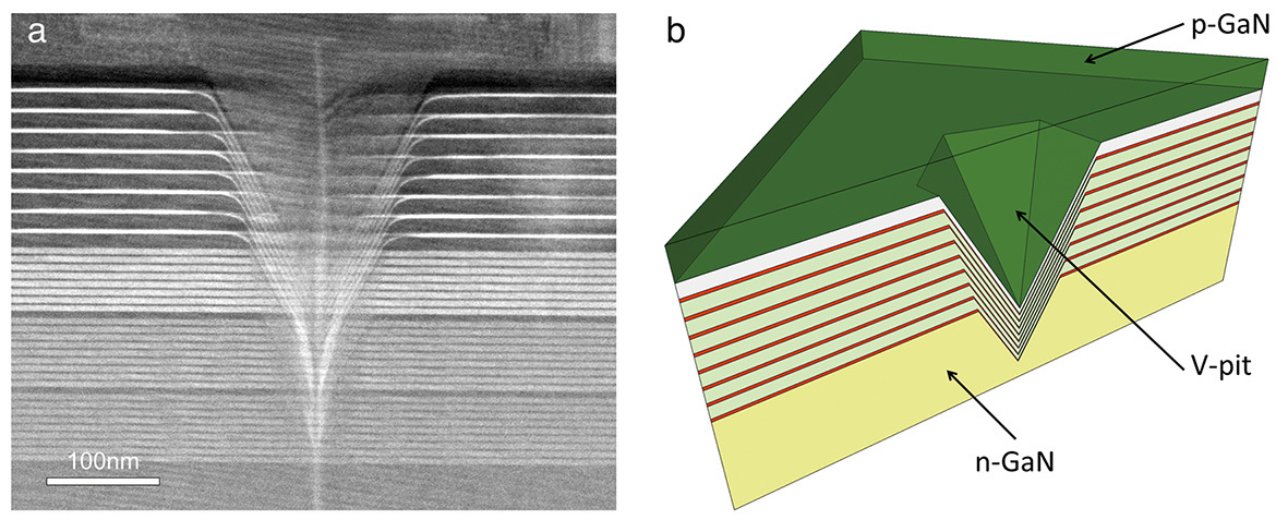
(a) TEM image of a V-pit and (b) schematic 3D PN junction with V-pit structure. (Image by JIANG’s group)
Shattering Records for Visible LEDs of Multi-Wavelengths
Armed with this novel 3D structure, the team rapidly shattered global efficiency records of LEDs with different wavelengths. For silicon-substrate GaN yellow LEDs, they drove the peak efficiency from less than 10% to 33.7%, and ultimately to a staggering 71% today.
The breakthroughs extended far beyond yellow light. The team also pushed the peak efficiency of silicon-substrate GaN green LEDs to above 70%, providing energy-saving solutions for specialized applications. In the highly challenging red spectrum, the peak efficiency of silicon-substrate GaN LEDs leaped from 2.5% to 16.8%, and now stands at 48%. This effectively overcomes the efficiency drop of traditional AlGaInP red LEDs at the micro-scale. The team now has successfully paved the way for silicon-substrate GaN blue, green, yellow, and red LEDs and silicon-based CMOS optoelectronic integration, laying the core technological groundwork for the future of the micro-display industry.
New Developments in the Semiconductor Lighting Industry
The industrial implications of this breakthrough are monumental. By enabling highly efficient, direct color-mixing white LEDs without the need for rare-earth phosphors, the team has created a new ecosystem of lighting. Their innovations have birthed high-quality light sources that directly improve daily life. For instance, they developed golden-yellow streetlights with advantages of warm color, strong permeability, high efficiency and long lifetime. Additionally, the team created dozens of “zero-blue-light” lamps that eliminate blue-light hazards during nighttime use, providing friendly light for bedtime. They also developed lighting products with infinitely adjustable dimming, which meet diverse demands of lighting.
Today, the V-defect 3D PN junction stands as one of the foundational technologies for phosphor and phosphor-free lighting materials, driving the development of the international semiconductor lighting and display industry with significant energy-saving and economic value.
Consensus and Application
Historically, the semiconductor lighting chip industry was dominated by the sapphire-substrate route. JIANG’s team single-handedly established the silicon-substrate GaN LED route, successfully building a comprehensive innovation ecosystem that spans equipment, materials, chips, packaging, and real-world applications.
Developed upon the silicon-substrate LED route, the theory and the method of V-defect 3D PN junctions have been extended and applied to the widely used sapphire-substrate LEDs. Professor Shuji Nakamura, a Nobel laureate in Physics, and his team have extensively cited JIANG’s works, noting:
“We have verified these results after receiving several packaged devices from Nanchang University… Jiang et al. from Nanchang University proposed a ‘3D PN junction’ from V-pits injection… The V-pits can screen the dislocations and increase the hole injection into the active region… This allows novel approaches for solving efficiency droop and achieving higher efficiency… The Nanchang LED group published a series of groundbreaking papers on yellow LEDs and red/orange LEDs grown on (111) Si… Nanchang University pioneered much of the early experimental work on V-defect engineered long-wavelength LEDs as well as some key simulation results… These results far exceeded other WPEs in the literature at the respective.”
Numerous international and domestic experts and enterprises have cited and applied the V-defect based 3D PN junction theory and method, significantly enhancing the efficiency of GaN-based red, yellow, green, and blue LEDs.
Reference
Jiang, F., Zhang, J., Xu, L., Ding, J., Wang, G., Wu, X., . . . Liu, J. (2019). Efficient InGaN-based yellow-light-emitting diodes. Photonics Research, 7(2), 144. doi: 10.1364/prj.7.000144
Zhang, S., Zhang, J., Gao, J., Wang, X., Zheng, C., Zhang, M., . . . Jiang, F. (2020). Efficient emission of InGaN-based light-emitting diodes: toward orange and red. Photonics Research, 8(11), 1671. doi: 10.1364/prj.402555